자료실
기술자료
THE EFFECT OF VACUUM REFLOW PROCESSING ON SOLDER JOINT VOIDING AND THERMAL FATIGUE RELIABILITY
ABSTRACT
A test program was developed to evaluate the effectiveness of vacuum reflow processing on solder joint voiding and subsequent thermal cycling performance. Area array package test vehicles were assembled using conventional reflow processing and a solder paste that generated substantial void content in the solder joints. Half of the population of test vehicles then were re-processed (reflowed) using vacuum reflow. Transmission x-ray inspection showed a significant reduction in solder voiding after vacuum processing. The solder attachment reliability of the conventional and vacuum reflowed test vehicles was characterized and compared using two different accelerated thermal cycling profiles. The thermal cycling results are discussed in terms of the general impact of voiding on solder thermal fatigue reliability, results from the open literature, and the evolving industry standards for solder voiding. Recommendations are made for further work based on other void reduction methods and additional reliability studies.
Key words : Solder joint voiding, vacuum reflow processing, thermal fatigue reliability, thermal cycling, lead-free alloys.
INTRODUCTION
The relationship between voiding and reliability of area array solder joints has been a topic of both study and debate for many years. The root cause of voids in solder joints is understood and has been documented in numerous publications on the topic [1-3]. There are industry guidelines for characterizing voiding [4, 5] but inspecting area arrays intrinsically is difficult and quantifying void content can be equally challenging.
The review of solder joint voiding by Aspandiar is a benchmark for discussion on this subject [3]. His analysis, summarized in Figure 1, shows that there are multiple types of voids and multiple void formation mechanisms. Voids can be differentiated with respect to how they are formed, where they reside in the solder joint and how they affect the reliability of the solder joint. Aspandiar further argues that during various types of stress testing such as temperature cycling, or mechanical shock and bending, cracks are more prone to initiate and propagate through these near-interfacial regions than in proximity to the geometric center of the solder joint. This hypothesis is illustrated in Figure 2a and Figure 2b.
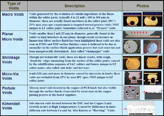
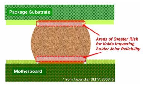
Figure 2a. Locations within a BGA solder joint where voids are expected to have a greater risk on joint reliability [3].
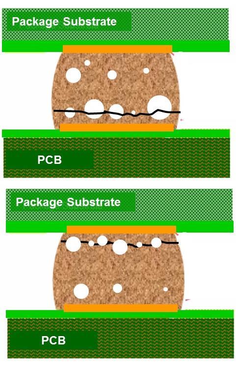
Figure 2b.Illustrations of void-assisted cracking at the PCB side (above) and package side (below) of the solder joints.
It is critical to understand if there is a correlation between area array solder joint voiding and the long term, thermal fatigue reliability of solder joints. Requirements for resistance to thermal fatigue are a priority for the products of many high reliability end users [6]. Solder joints age and degrade during service and eventually fail by the wear out mechanism of thermally activated solder fatigue (creep fatigue) [7], which is the major wear-out failure mode and major source of failure for surface mount (SMT) componentsin electronic assemblies [8].
A specific type of voiding called planar microvoiding has been shown to lower reliability either by effectively reducing the attachment area or by weakening the solder in regions of the solder joint where cracks tend to propagate [9]. This effect is illustrated by the Weibull plot in Figure 3, in which planar microvoiding reduces the characteristic lifetime eta (thermal fatigue reliability) by 23%. The photomicrographs taken from orthogonal cross sections of failed thermal cycling samples show that microvoiding and its effects on crack propagation are not always evident or easy to detect using standard failure analysis techniques. A similar effect due to planar voiding was reported for mechanical reliability testingperformed by Mukadam et al [10]. Planar microvoiding however, is a specialized case of voiding most often associated with surface finish issues or surface contamination.
Such a clear correlation has not been established between process macro voiding and decreased reliability. Aspandiar points out that the current industry position states that macrovoids do not affect solder joint reliability [3]. That position is supported by results from several studies in which macrovoids did not reduce board level reliability [11-13]. Independent investigations by Sethuraman [14], Coyle [15], and Hillman [16]] found that the presence of a voids was not necessarily sufficient to lower solder joint reliability. Rather, the location of void relative to the solder joint failure crack path has a much larger impact than the existence of the void alone.
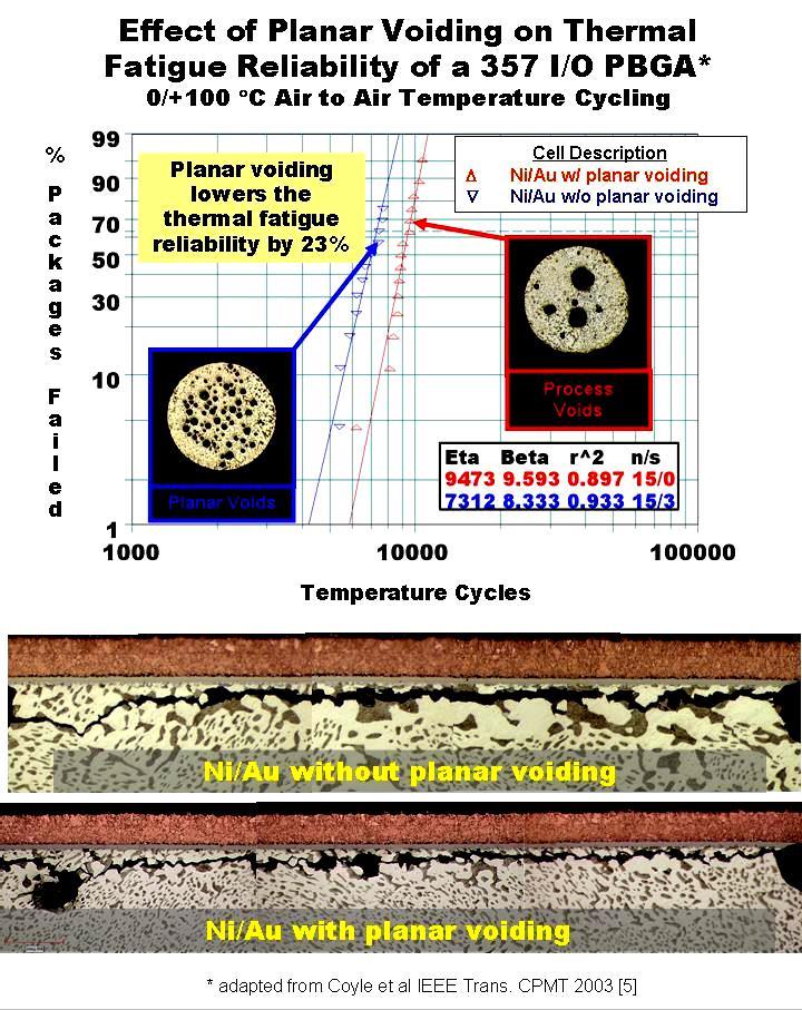
Figure 3. The Weibull plot illustrates the influence of planar microvoiding on thermal fatigue reliability. The imbedded planar or flat section photomicrographs show the reduction in solder joint attachment area caused by planar voiding. The lower photomicrographs are fatigue failures that show that the planar microvoiding is not always obvious in orthogonal cross sections [9].
Because a finished electronic assembly can be rejected based on the IPC guidelines for macro or process voiding defects[4, 5], it is desirable to eliminate voiding, or least reduce thevoid density substantially. Various process techniques have been employed to reduce voiding including reflow profile modifications, nitrogen atmosphere reflow, and implementation of special solder paste formulations andstencil designs [17]. Despite attempts to optimize processes and minimize voiding, a certain amount of solder joint voiding in typical surface mount assemblies is considered inevitable.
Vacuum reflow is an acknowledged process option for reducing void density in solder joints. However, Sweatman et al showed that vacuum reflow by itself does not ensure a void-free solder joint [18]. Thus even with vacuum reflow, the debate remains regarding the effect of voiding on solder joint reliability. This paper reports the results from a test To be published in the Proceedings of SMTA International, September 17 - 21, 2016, Rosemont, IL.program designed to evaluate the effectiveness of vacuum reflow processing on solder joint voiding and on thermal fatigue reliability of the solder joints measured by thermal cycling. The thermal cycling results are discussed in terms of the general impact of voiding on solder thermal fatigue reliability, results from the open literature, and the evolving industry standards for solder voiding.
EXPERIMENTAL
Component and Test Board Description
The printed circuit board (PCB) test vehicle and components, shown in Figure 4, was developed originally for the iNEMI Alloy Alternatives study [19].
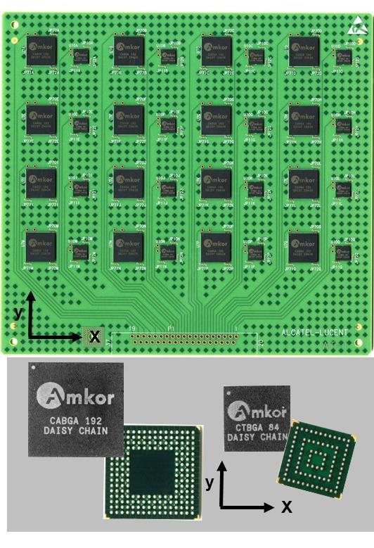
Figure 4. A populated printed circuit board test vehicle.
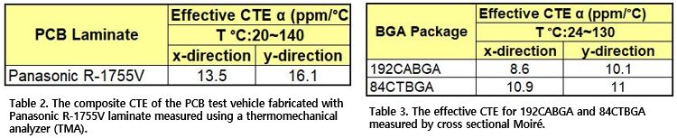
The test boards were populated with daisy-chained 192CABGA and 84CTBGA packages fabricated with Pbfreesolder spheres. The printed circuit board (PCB) test vehicle is 2.36 mm (93 mils) thick, with a 6 layer construction and 16 sites each for the 192CABGA and 84CTBGA. The test boards were fabricated with Panasonic R-1755V high temperature PCB laminate and Entek HT Plus organic solderability preservative (OSP) final finish. The component and PCB attributes are shown in Table 1.
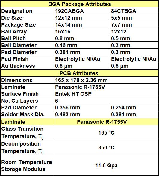
Table 1. 192CABGA, 84CTBGA, and printed circuit board test vehicle attributes.
Test Vehicle Surface Mount Assembly
The test boards were assembled using a conventional reflow process with a nominal peak reflow temperature of 250°Cand a nominal measured time above liquidus of 60 seconds. The Pb-free solder paste used for assembly generatedsubstantial void content in the solder joints. Subsequently, half of the population of test vehicles were re-processed using vacuum reflow to reduce the voiding.
The vacuum assisted reflow was performed in a 15-zone convection reflow oven with 3 convection cooling zones. The vacuum oven is located between heating zone 15 and cooling zone 1. The peak temperature was 238°C, and the time above liquidus (217°C), and soak time for the re-assembly reflow were 80 seconds and 65 secondsrespectively. The convection zone set points are depicted in Table 2 for this re-assembly reflow process. The vacuum reflow chamber IR Panel heater was set to 300 °C for this process.
| Zone | Top(℃) | Bottom(℃) | Zone | Top(℃) | Bottom(℃) | |
| 1 | 190 | 190 | 9 | 200 | 200 | |
| 2 | 200 | 200 | 10 | 200 | 200 | |
| 3 | 200 | 200 | 11 | 200 | 200 | |
| 4 | 200 | 200 | 12 | 240 | 240 | |
| 5 | 200 | 200 | 13 | 255 | 255 | |
| 6 | 200 | 200 | 14 | 265 | 265 | |
| 7 | 200 | 200 | 15 | 265 | 265 | |
| 8 | 200 | 200 |
Table 2. Convection reflow heat zone set points for the reassembly reflow process.
The vacuum reflow profile for the re-assembly process is shown in Figure 5. The red rectangle denotes the total time the substrates were in the vacuum chamber, which is approximately 60 seconds. This total time includes transport of the test vehicles in and out of the vacuum chamber as well as pump down, refill and dwell times. The pump down time is 8 seconds, the dwell time at 10 torr vacuum is 20 seconds,and the refill time is approximately 5 seconds. The peak temperature in the reflow profile is achieved while the substrates are in the vacuum chamber under IR Panel heating.
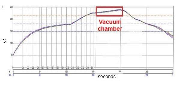
Figure 5. Vacuum reflow profile used in the re-assembly process. The total time in the vacuum chamber, outlined by the red rectangle, is 60 seconds. The vacuum dwell time at 10 torr is 20 seconds.
The vacuum chamber located within the convection reflow oven is shown in Figure 6 with the vacuum doors open, ready to receive a substrate.
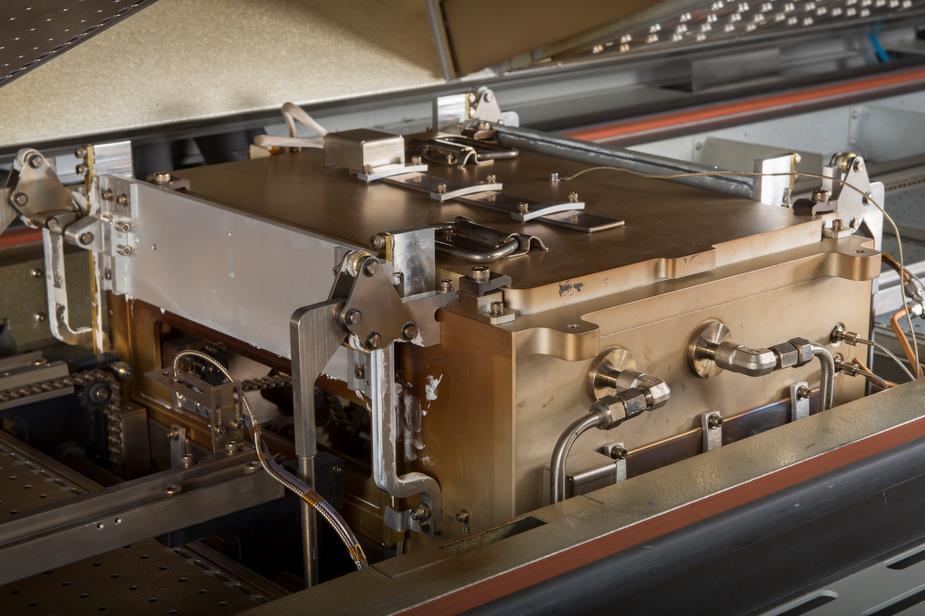
Figure 6. Vacuum reflow chamber shown within the convection reflow oven.
CTE Measurements
Solder joint attachment reliability is dependent strongly on the coefficient of thermal expansion (CTE) mismatch between the package and the PCB [20, 21]. The CTE of the PCB was measured using a thermomechanical analyzer (TMA) and the composite coefficients of thermal expansion of the 192CABGA and 84CTBGA packages were measured using microscopic Moiré interferometry. The CTE data for the PCB and the two BGA components are shown in Table 2 and Table 3.
Accelerated Temperature Cycling
The daisy-chained components and the test circuit boards enabled electrical continuity testing after surface mount assembly and in situ, continuous monitoring during thermal cycling. Thermal cycling was done in accordance with the IPC-9701A guideline [22]. The solder joints were monitored using an event detector set at a resistance limit of 1000 ohms. The failure data are reported as characteristic life(the number of cycles to achieve 63.2% failure) and slope from a two-parameter Weibull analysis.
The two accelerated temperature cycling profiles are shown in Table 4. These profiles are associated most often with the reliability requirements for telecommunications, represented by 0/100 °C (TC1), and requirements for military/defenserepresented by -55/125 °C (TC4) [22].
Table 4. Thermal Cycling Profiles.
Experimental Test Matrix
The components and thermal cycling profiles are shown in Table 5. Each test cell contains replicate fully populated test boards to provide an initial sample size of 32 192CABGA and 32 84CTBGA components. Additional samples were assembled for baseline quality and microstructural characterization.
Table 5. Component samples sizes for the accelerated temperature cycling test matrix.
Solder Joint Void Characterization and Failure Analysis
Transmission x-ray inspection and metallographic cross sectional analysis were used to characterize solder joint voiding and time-zero microstructures of representative board level assemblies. The baselines document the time zerocondition to enable comparisons to samples removed from the temperature cycling chambers for failure analysis. The solder joint quality and microstructure were documented using optical and scanning electron microscopy. The SEM was operated in the backscattered electron imaging (BEI) mode to differentiate phases in the Pb-free microstructure.
RESULTS
Solder Joint Void Characterization
The factory x-ray inspection on the conventional or standard SMT (STD SMT) reflow assembly revealed substantial void content in the BGA solder joints of both components. The xrayimages in Figure 7a (192CABGA) and Figure 8a (84CTBGA) are typical of the extent and size of the solder voids. Note that the largest voids result in a noticeable increase in the diameter of the solidified solder spheres.
Half of the population of voided test vehicles was subjected to secondary assembly using vacuum reflow processing to reduce the voiding. The x-ray images in Figure 7b (192CABGA) and Figure 8b (84CTBGA) show the resultant solder joint quality after vacuum reflow. In the expanded xrayimages (identified as STD SMT + VAC SMT), there is no indication of solder voiding in either component aftervacuum reflow processing.
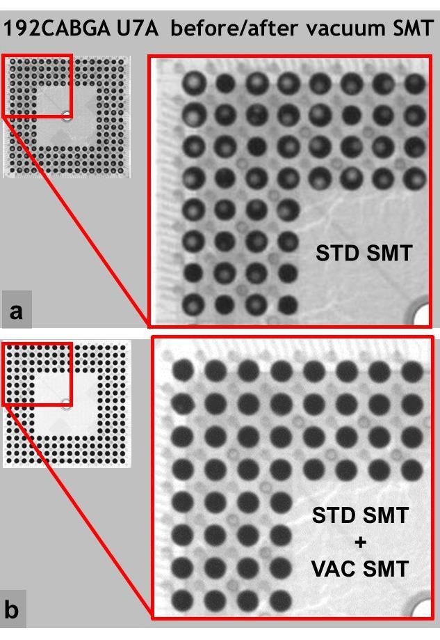
Figure 7. Transmission x-ray images of a) a typical heavily voided 192CABGA after SMT assembly and b) the same 192CABGA with solder voiding eliminated by subsequent vacuum reflow processing.
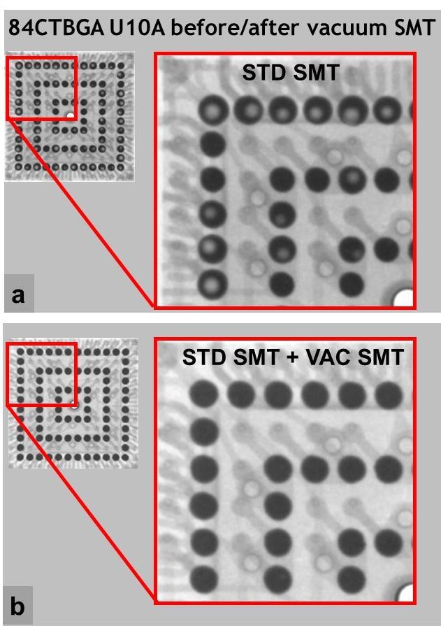
Figure 8. Transmission x-ray images of a) a typical heavily voided 84CTBGA after SMT assembly and b) the same 84CTBGA with solder voiding eliminated by subsequent vacuum reflow processing.
Cross sectional views of the voiding are shown in the optical photomicrographs in Figure 9. Many of the voids observed in the cross-sectional analysis exceed the IPC-JSTD-001 BGA maximum void criteria of 30% of the X-ray image area [23]. This observation is supported qualitatively by the noticeable increase in the diameter of the solidified solder spheres shown in the x-ray images in Figure 7.
In comparison to the planar x-ray images in Figures 8 and 9, cross sectional images can show the position of the void relative to the soldered interfaces where fatigue cracks are expected to propagate (see Figure 2). Because the voiding is not always centered in the solder sphere or on the pads (see x-ray images), cross sectional images may not represent the size of the voids accurately. In the worst case, an offset void may not appear at all in a cross sectional image. However, some of the images in Figure 9 illustrate the risk of void location at a soldered interface, thereby increasing the risk of earlier failure in thermal cycling. For failure analysis, cross sectional images can be used compliment the x-ray images, but destructive cross sectioning obviously cannot be used to characterize samples before they are placed into thermal cycling.
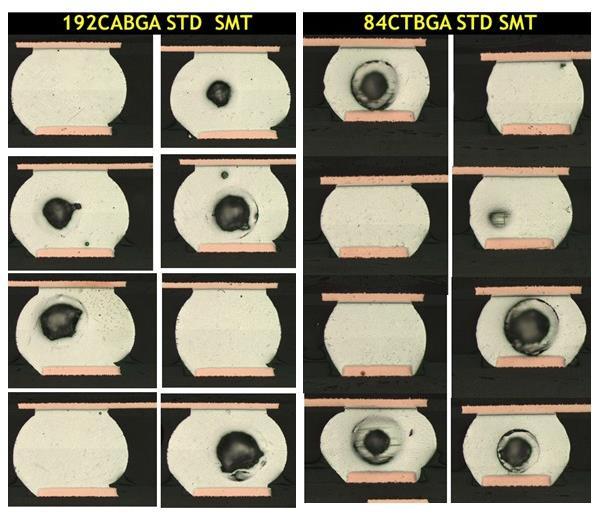
Figure 9. Optical photomicrographs showing a variety of solder joint voids and void locations in the 192CABGA and 84CTBGA components. Note, the voids in some solder joints are located near a soldered interface where fatigue cracks propagate (shown schematically in Figure 2b), thereby increasing the risk of earlier failure in thermal cycling.
Thermal Cycling
Figure 10 and Figure 11 are Weibull distribution plots from the 0/100 °C and -55/125 °C thermal cycling tests respectively. Table 6 provides a summary of the Weibull statistics for those two tests.
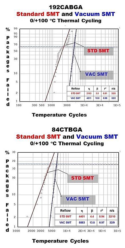
Figure 10. The Weibull distribution plots for the 192CABGA and 84CTBGA packages from the 0/100 °C thermal cycling showing the improved reliability aftereliminating voiding with vacuum SMT processing.
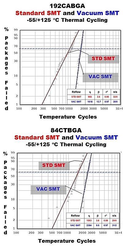
Figure 11. The Weibull distribution plots for the 192CABGA and 84CTBGA packages from the -55/125 °C thermal cycling showing the improved reliability after eliminating voiding with vacuum SMT processing.
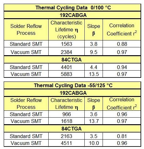
Table 6. Summary of Weibull statistics for the 192CABGA and 84CTBGA packages with and without vacuum processing.
The thermal cycling results show a clear improvement in characteristic lifetime (reliability) and Weibull slope (data quality) with vacuum processing. Although BGA solder joint voiding very often does not present an attachment reliability To be published in the Proceedings of SMTA International, September 17 - 21, 2016, Rosemont, IL.risk [14-16], the large size and the location of voiding in the current samples affects the failure process during thermal cycling. Additionally, it is reasonable to assume that variations in voiding within individual samples and across the sample sets account for the lower Weibull slopes.
Failure Analysis
The -55/125 °C thermal cycling test started substantially after the 0/100 °C test, and only samples from the 0/100 °C cycle were available for failure analysis at the time of this writing. Examples of void-assisted solder joint failures from the TC1 0/100 °C thermal cycling test are shown in the optical photomicrographs in Figure 12. The large solder voids reduce the effective attachment area through which the crack propagates, thereby reducing the number of cycles to failure. The failure mode remains solder fatigue, and the reduction in fatigue life is attributed to the geometric effect of reducing the crack path. These samples are two of the earliest failuresin the 0/100 °C thermal cycling test, and it certainly is reasonable to assume that the earlier failure is related to the immense size of the voids.
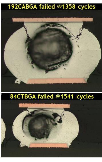
Figure 12. Optical photomicrographs showing void-assisted solder joint failures after in 0/100 °C thermal cycling for the 192CABGA and 84CTBGA (STD SMT).
The optical photomicrographs in Figure 13 show examples of solder joint failures (0/100 °C thermal cycling) in samples that were vacuum processed. These images show bulk soldercracking characteristic of thermal fatigue in SAC alloys. In the 192CABGA package, the failures occur mostly at the PCB side of the solder joints, with some fatigue crack initiation is found at the package side. Although package-side solder joint failures are typical in BGA thermal cycling experiments, PCB-side failures are known to occur with this 192CABGA package [24]. The fatigue failures in the 84CTBGA package are found in the bulk solder at the package-side location more typical for BGA fatigue cracking.
The metallographic images of components that failed during thermal cycling confirm the findings from the Weibull analysis summarized in Table 6 and are in agreement with the IPC-JSTD-001 maximum void criteria. It is clear that vacuum reflow has remediated the solder process voiding and likewise remediated the thermal fatigue reliability of the solder. When the voiding is extremely large and occupies a position in the potential fatigue crack path, the reduction in characteristic lifetime caused by void-assisted fracture of the solder joint is between 25 and 50%. This relationship between solder joint life, voiding, and the absence of voiding has been demonstrated dramatically using two different components and two different thermal cycling profiles.
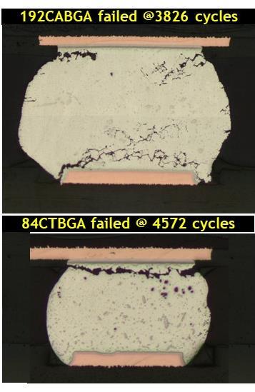
Figure 13. Optical photomicrographs showing solder joint fatigue failures in the 192CABGA and 84CTBGA packages. The thermal cycling profile was 0/100 °C.
FUTURE WORK
The -55/125 °C test was nearing completion at the time of this writing, but there was not enough time to complete the failure analysis of samples from that thermal cycling profile.The failure analysis and characterization for the -55/125 °C thermal cycling profile will be reported later. Based on the Weibull statistics the failure analysis is expected to yield results consistent with observations from the 0/100°C test.
The thermal cycling results show a clear improvement in characteristic lifetime (reliability) and Weibull slope (data quality) with vacuum processing. However, the basis of the current study is remediation of voiding in existing solder joints, which can be described as a rework process at the To be published in the Proceedings of SMTA International, September 17 - 21, 2016, Rosemont, IL.board level. End users that struggle with voiding that exceeds specifications would prefer to eliminate voiding during the initial reflow, rather than rework the voided product. To strengthen the comparison, it would be valuable to evaluatethe solder joint assembly quality of boards where the initial SMT assembly was done using vacuum reflow and the paste from the current study that generated voiding.