Products
Giới thiệu sản phẩm
Elec-Beam Machinery
X-eye NF120
작성자 관리자
날짜 2023-07-24 15:34:41
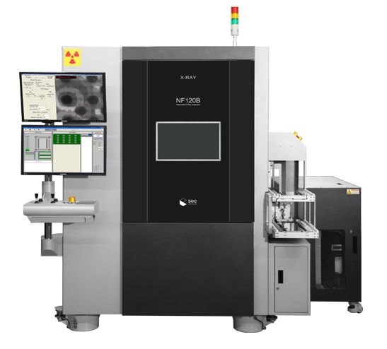
Nano-focus Tube of 200 nano resolution is installed which is specialized for Semiconductor Packaging, Wafer Level Packaging(WLP)
requiring detection of Sub-micron defect. Able to trace and inspect defected area precisely by precise movement of axis with Antivibration
table. Tomography is available if 3D CT module is added and Wafer Bump Automatic Inspection is available from loadeing
to inspection with wafer handler systems.
- Non-destructive analysis system for Wafer Level Packaging
- High resolution image with Dual Type CTs
- TSV, Micro Bump, Patterm
| General Product Features | |
|---|---|
| X-ray Tube | 120kv / 200㎂ |
| Min Resolution | 0.2㎛ |
| Table Size | 12 inch Wafer |
| AXIS | X, Y, Z Tilt(70º), R |
| Detector | 6 inch FPXD |
| CT Scan 방식 | Oblique CT / Cone beam CT |
| Dimensin | 2,380(W) x 1,450(D) x 2,120(H)mm / 7,000kg |
X-ray Image
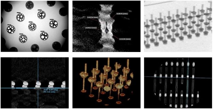
고해상도 이미지
댓글 (0)
등록된 댓글이 없습니다.